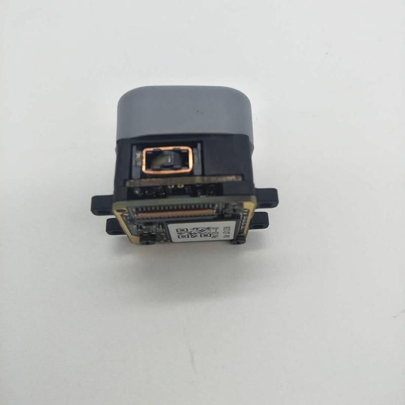
M256 uncooled thermal imaging module

♦ Introductions
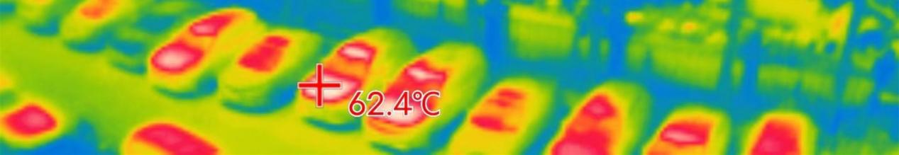
Thermal imaging module is based on ceramic packaging uncooled vanadium oxide infrared detector to develop a high performance infrared thermal imaging products, the products adopt parallel digital output interface, interface is rich, adaptive access a variety of intelligent processing platform, with high performance and low power consumption, small volume, easy to the characteristics of the development integration, can meet the application of various kinds of infrared measuring temperature of secondary development demand.
Product features
- The product is small in size and easy to integrate;
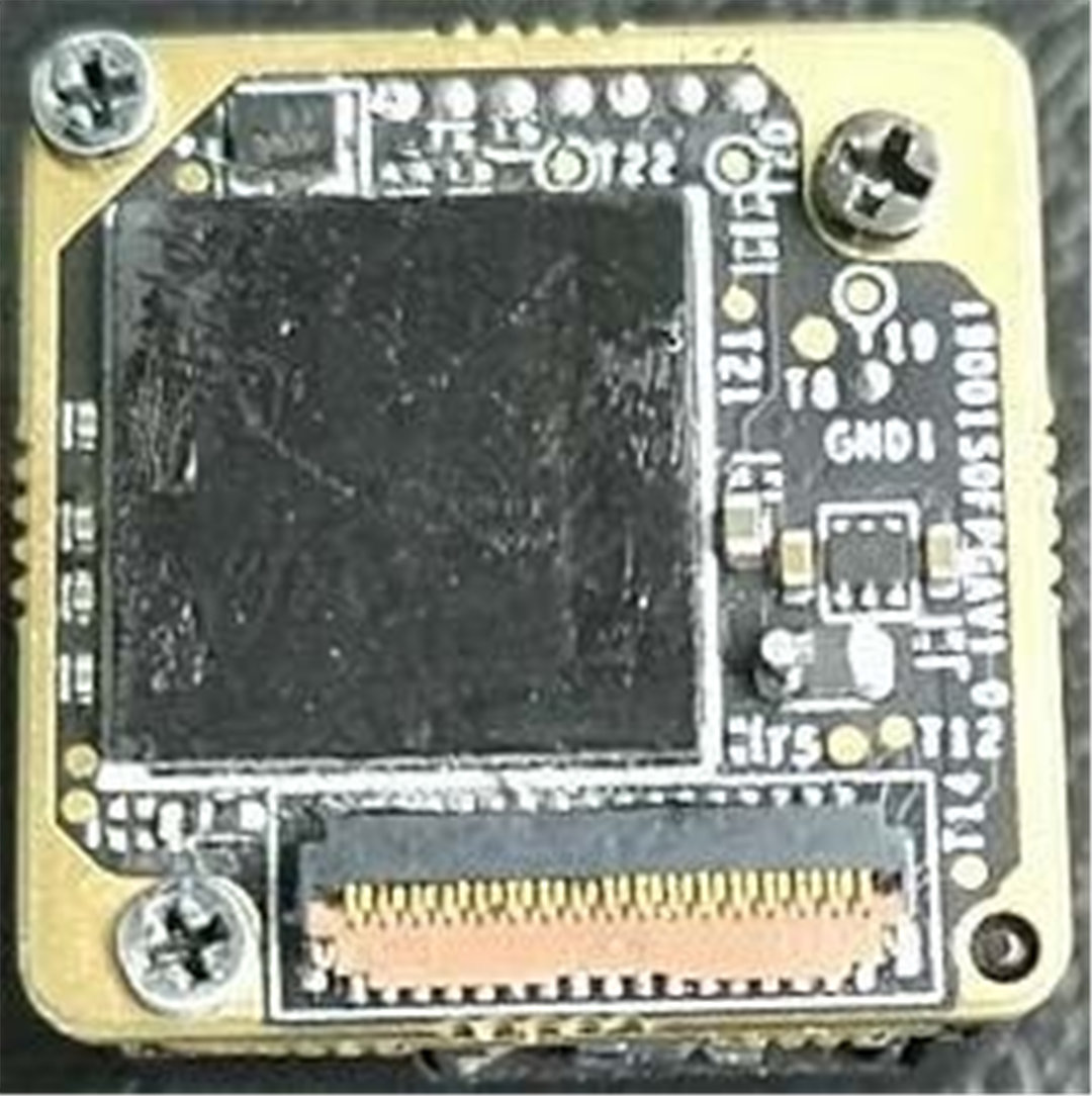
- FPC interface is adopted, which is rich in interfaces and easy to connect with other platforms;
- Low power consumption;
- High image quality;
- Accurate temperature measurement;
- standard data interface, support secondary development, easy integration, support access to a variety of intelligent processing platform.
♦ product paremeters
| Type | M256 | |
| Resolution | 256×192 | |
| Pixel space | 12μm | |
| FOV | 42.0°×32.1° | |
| FPS | 25Hz/15Hz | |
| NETD | ≤60mK@f#1.0 | |
| Working temperature | -15℃~+60℃ | |
| DC | 3.8V-5.5V DC | |
| Power | <200mW* | |
| Weight | <18g | |
| Dimension(m m) | 20*20*21 | |
| Data interface | parallel/USB | |
| Control interface | SPI/I2C/USB | |
| Image intensification | Multi-gear detail enhancement | |
| Image calibration | The shutter correction | |
| Palette | White glow/black hot/multiple pseudo-color plates | |
| Measuring range | -10℃~+50℃(customized up to | |
| 500℃) | ||
| Accuracy | ±0.5% | |
| Temperature correction | Manual | |
| /Automatic | ||
| Temperature statistics output | Real-time parallel | |
| output | ||
| Temperature measurement statistics | Support maximum /minimum statistics,temperature analysis | |
| Paralles interface in 25Hz output mode. | ||
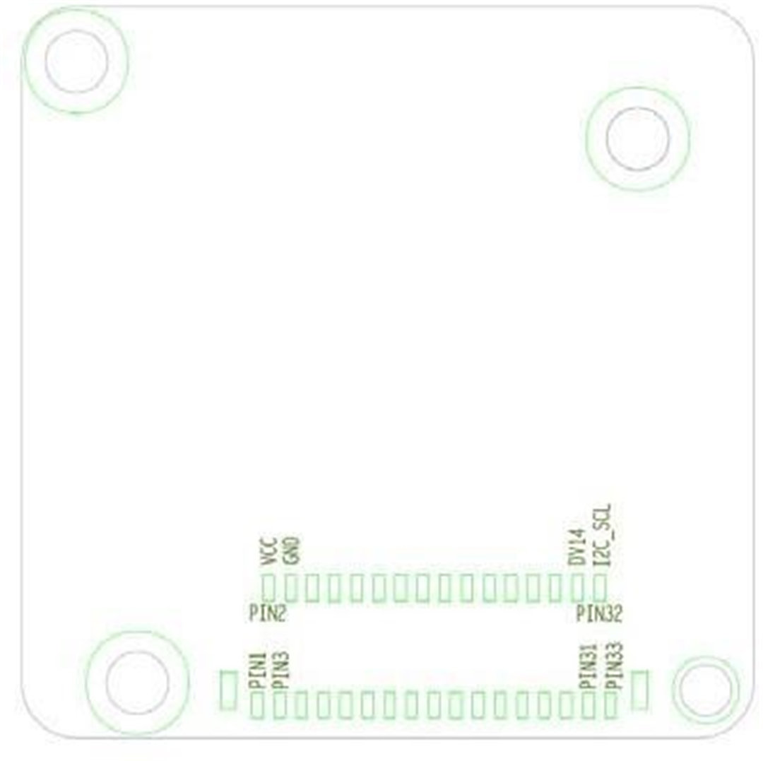
| User interface description | ||
| The product adopts 0.3Pitch 33Pin FPC connector (FH26W-33S-0.3SHW(97)), and the input voltage is: | ||
| 3.8-5.5VDC, undervoltage protection is not supported. | ||
♦ Specification
Form 1 interface pin of thermal imager
| Pin number | name | type | voltage | Specifi cation | |
| 1,2 | VCC | Power | -- | power | |
| 3,4,12 | GND | Power | -- | floor | |
| 5 | USB_DMj | I/O | -- | USB 2.0 | DM |
| 6 | USB_DPj | I/O | -- | DP | |
| 7 | USBEN*k | I | -- | USB enabled | |
| 8 | SPI_SCK | I | Default:1.8V | SCK | |
| 9 | SPI_SDO | O | LVCMOS ; | SDO | |
| 10 | SPI_SDI | I | ( if need 3.3V | SPI | SDI |
| 11 | SPI_SS | I | LVCOMS output, please contact us) | SS | |
| 13 | DV_CLK | O | CLK | ||
| 14 | DV_VS | O | VS | ||
| 15 | DV_HS | O | HS | ||
| 16 | DV_D0 | O | DATA0 | ||
| 17 | DV_D1 | O | DATA1 | ||
| 18 | DV_D2 | O | DATA2 | ||
| 19 | DV_D3 | O | DATA3 | ||
| 20 | DV_D4 | O | DATA4 | ||
| 21 | DV_D5 | O | DATA5 | ||
| 22 | DV_D6 | O | DATA6 | ||
| 23 | DV_D7 | O | DATA7 | ||
| 24 | DV_D8 | O | DATA8 | ||
| 25 | DV_D9 | O | DATA9 | ||
| 26 | DV_D10 | O | DATA10 | ||
| 27 | DV_D11 | O | VIDEOl | DATA11 | |
| 28 | DV_D12 | O | DATA12 | ||
| 29 | DV_D13 | O | DATA13 | ||
| 30 | DV_D14 | O | DATA14 | ||
| 31 | DV_D15 | O | DATA15 | ||
| 32 | I2C_SCL | I | I2C | SCL | |
| 33 | I2C_SDA | I/O | SDA | ||
Pin5, Pin6 default USB2.0, compatible with 3.3 V TTL UART interface for UART interface please
contact us.Note: Pin5: TX;Pin6: RX; TX, RX phase Xmodule S0;
k USB_EN pins 5 and Pin5, Pin6 default USB2.0, compatible with 3.3 V TTL UART interface for UART interface please
6 pin high levels as the USB data pins, USB communication USES the UVC communication protocol, image formats to YUV422 for USB communication development kit please contact us;
l in PCB design, parallel digital video signal suggested 50 Ω impedance control.
Form 2 Electrical specification
Format VIN =4V, TA = 25°C
|
Parameter |
Identify |
Test condition |
MIN TYP MAX |
Unit |
|
Input voltage range |
VIN | -- |
3.8 4 5.5 |
V |
|
Capacity |
ILOAD | USBEN=GND |
75 300 |
mA |
| USBEN=HIGH |
110 340 |
mA | ||
|
USB enabled control |
USBEN-LOW | -- |
0.4 |
V |
| USBEN-
HIGN |
-- |
1.4 5.5V |
V |
Form 3 Absolute Maximum rating
| Parameter | Range |
| VIN to GND | -0.3V to +6V |
|
DP,DM to GND |
-0.3V to +6V |
| USBEN to GND | -0.3V to 10V |
| SPI to GND | -0.3V to +3.3V |
|
VIDEO to GND |
-0.3V to +3.3V |
| I2C to GND | -0.3V to +3.3V |
|
Storage temperature |
−55°C to +120°C |
|
Working temperature |
−40°C to +85°C |
Note: Ranges listed that meet or exceed absolute maximum ratings may cause permanent damage
to the product.This is just a stress rating;Don't mean that the functional operation of the Product
under these or any other conditions is higher than those described in the operations section of this
specification. Prolonged operations that exceed maximum working conditions may affect the
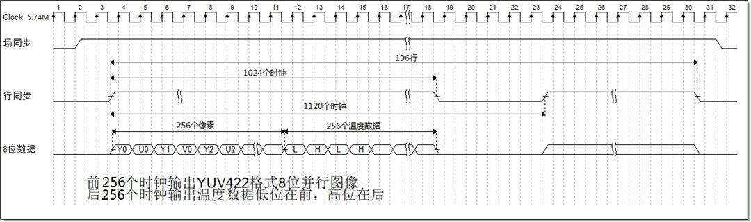
digital interface output sequence diagram
Figure3 8bit parallel image
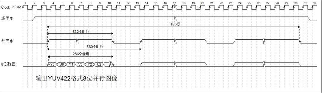
Figure4 :8bit parallel image and temperature
when use 8bit parallel output interface,default output interface is DV_D0~DV_D7
Figure 5: 16bit parallel image data
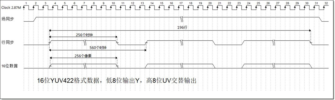
Figure 6 :16bit parallel image and temperature data
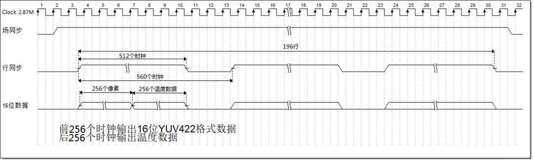
Attention:(1)The data is recommended to be sampled at the rising edge of Clock;
(2) Field synchronization and line synchronization are both highly effective;
(3) Image data format is YUV422,Data low value is Y,high value is U/V;
(4) The temperature data unit is(Kelvin(K)*10),actual temperature is read-out value /10-273.15(℃)。
♦ Attention
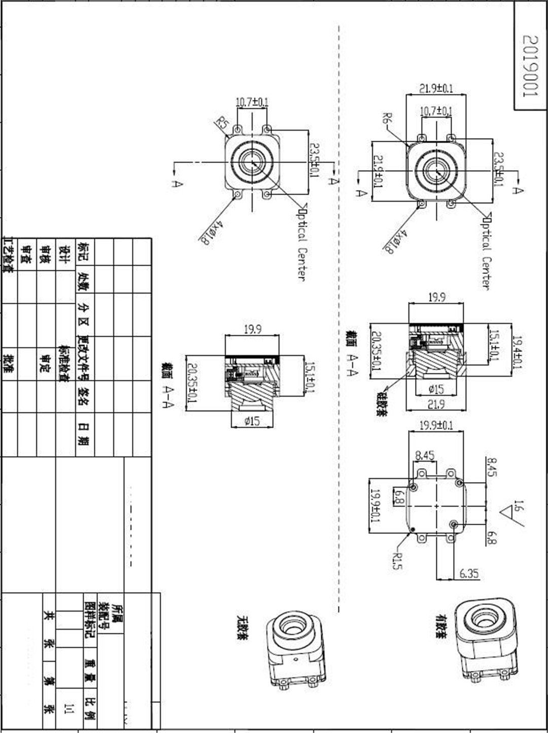
appendix 2 Figure 8 Mechanical interface dimension
To protect you and others from injury or to protect your device from damage, please read all of the following information before using your device.
- Do not look directly at the high-intensity radiation sources such as the sun for the movement components;
- Do not touch or use other objects to collide with the detector window;
- Do not touch the equipment and cables with wet hands;
- Do not bend or damage the connecting cables;
- Do not scrub your equipment with diluents;
- Do not unplug or plug other cables without disconnecting the power supply;
- Do not connect the attached cable incorrectly to avoid damaging the equipment;Please do not disassemble the equipment. If there is any fault, please contact our company for professional maintenance.
- Please pay attention to prevent static electricity;
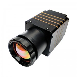
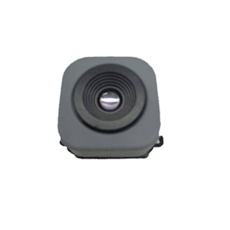
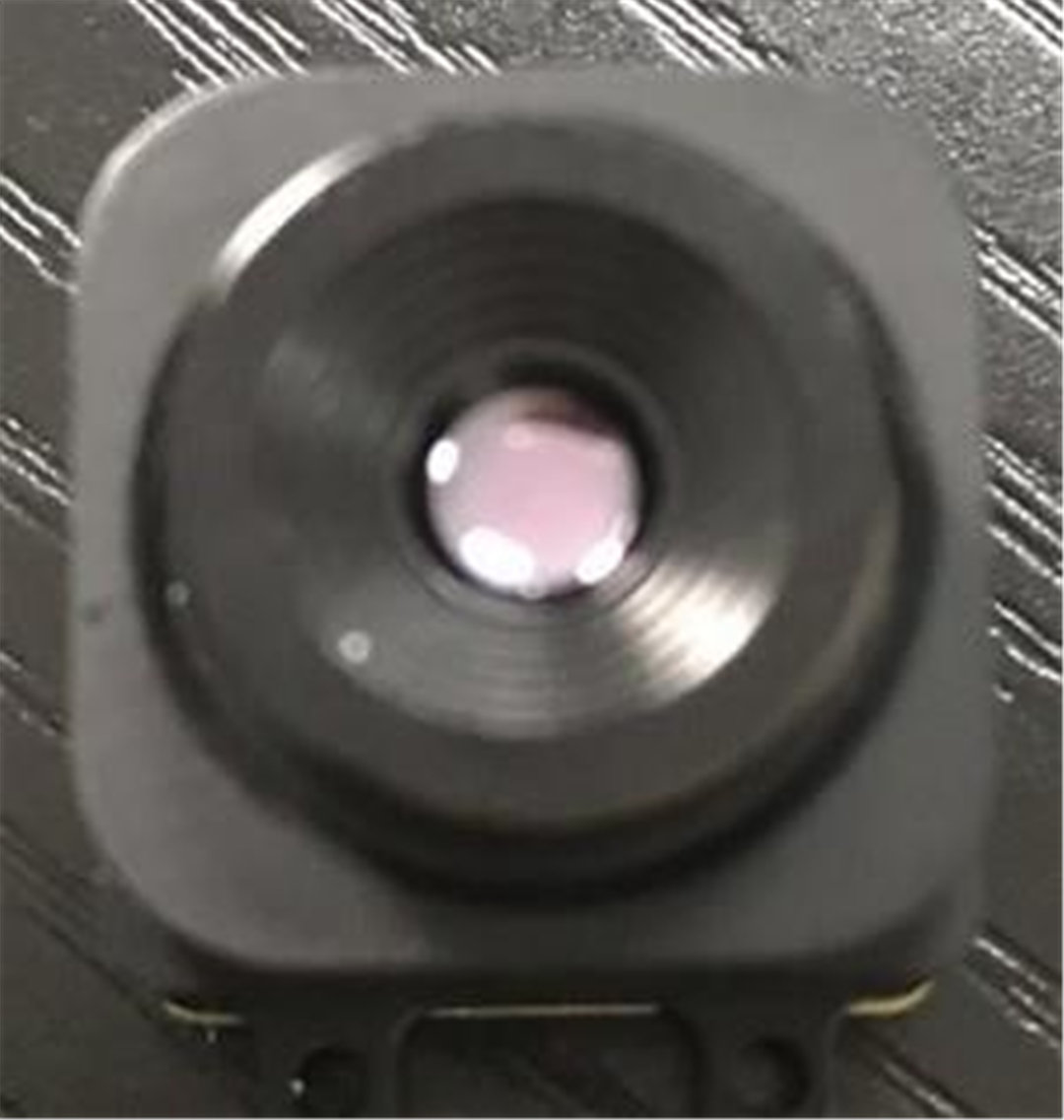
appendix1 product view
Figure 7 product front view(positive direction):
appendix 3 I2C control protocol
chart 3 module I2C address 7bit device address(0x18),read address 0x31, write address 0x30。
| number | Register address | parameter | description |
| 1 | 0x00 | shutter correction * | |
| 2 | 0x01 | background correction | |
| 3 | 0x02 | Detector original output | |
| 4 | 0x05 | Image data output | |
| 5 | 0x20 | Temperature measurement at normal temperature section | |
| 6 | 0x21 | Temperature measurement at extend temperature section | |
| 7 | 0x27 | 16-bit parallel image output | |
| 8 | 0x28 | 8 -bit parallel image output | |
| 9 | 0x80 | 0x29 | 16 -bit parallel image +temperature data output |
| 10 | 0x2A | 8-bit parallel image +temperature data output | |
| 11 | 0x2B | Load temperature parameters | |
| 12 | 0xFE | Save configuration parameters | |
| 13 | 0x88 | 0-7 | pallete |
| 14 | 0x96 | float type | Target reflection temperature(default |
| 25℃) | |||
| 15 | 0x97 | float type | Target ambient temperature(default |
| 25℃) | |||
| 16 | 0x98 | float type | ambient temperature(default 0.45) |
| 17 | 0x99 | float type | Target emissivity (default 0.98) |
| 18 | 0x9a | short type | Target distance (default: 1m) |